Appendix_1_Depreciated
Over the course of the multi-year cloudSmoker project, my design changed as problems were encountered, eventually solved and the design further optimised. At times, I chose to abandon a design element that I had spent a lot of time on; an example being dropping a number of design solutions to the on-board esp8266 ADC by switching to an external ADS1015 ADC module.
These design dead-ends represent discarded work, but perhaps will be useful to me (or others) in future projects. As such, this Appendix preserves the design work write-ups for the discarded project elements.
One of the many ESP8266 challenges are the limited number of pins, including a single ADC pin and only six available GPIO pins (for ESP-07/12 modules; there are even less pins on other modules). In general, the other pins are used for start-up or IC operations.
GPIO pins 6 to 11 are used to connect to flash memory and therefore not available for use, leaving nine remaining GPIO pins on the ESP-07/12 modules. However, three of these pins are needed for start-up / reset functions as shown in the table below:

This essentially leaves six GPIO pins completely free for general use.
This limited number of pins initially presented some issues to me as I considered my project design, where, after iterating through a number of ideas, I still required a total of seven GPIO pins for this project to:
-
Read at least two thermistors into the single ADC (solution: multiplexing, at the cost of using two GPIO pins);
-
Connect to a 16x2 LCD display (solution: I2C, requiring another two GPIO pins); and
-
Have some sort of means for LCD menu control and data entry (solution: rotary encoder with button switch, requiring an additional three GPIO pins)
At the end of the day, finding seven available pins required that I re-use two of the pins that are initially required for startup (GPIO0 and GPIO2). I discovered the solution in this useful blog post: ESP8266_01 Pin Magic where the author showed how GPIO0 and GPIO2 could be used for both start-up functions and subsequently also the I2C bus lines. A similar solution is also discussed in this Instructable.
I2C Design Note: Before using I2C, pins for SDA and SCL need to be set (defined) on the ESP module by calling Wire.begin(int sda, int scl), i.e. Wire.begin(0, 2), else they default to pins 4(SDA) and 5(SCL). Reference: Esp8266 Arduino Core Documentation - I2C (Wire Library)
Note: The decision to move to an external I2C ADS1015 ADC module with four analog pins (internally multiplexed) meant that I no longer was analog pin limited on the ESP8266
One issue with the ESP8266 is that it only has a single 10-bit ADC pin, yet my project design requires two or three analog temperature sensors as discussed in the previous section. At first I thought this might force me back to the Arduino solution (which has multiple analog pins) when I stumbled across multiplexing as a solution. Multiplexing allows me to combine multiple analog signals into a single signal.
There are a number of multiplexer chips available. I ended up buying TI's CMOS 4066B Quad Bilateral Switch which can also be configured for mux / demux applications for up to four different analog signals (datasheet info). The 4066B uses a digital control pin to "turn on/off" a switch across two analog input/output pins as shown in the diagram. In retrospect, I'm not completely sure that this chip was the best choice for multiplexing. On the positive side, switching between analog signals is easy by using software to instruct the ESP8266 to pull the respective 4066B control pin high to turn on the analog pin. On the negative side, the lower the voltage, the higher the pin impedance becomes. For my case using 3.3V, the datasheet indicates impedance could be as high as 250 ohms. I'll investigate whether that causes me any issues but was encouraged after seeing online reports suggesting it works at 3.3V. ***Alternatively, power at 5V (5V rail)?

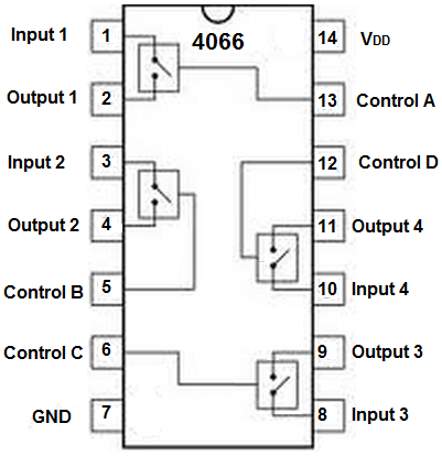
Note that the datasheet recommends not to float unused inputs, therefore all unused pins (particularly controlpins) need to be pulled low, in my case the unused control pin for switches C & D (pins 6 & 12).
An alternative approach is to bypass the ESP8266 ADC and the single analog input pin completely by using an external ADC such as the ADS1115, which is available as a low cost breakout board module, having
- 16 bit ADC
- 4 analogue channels or 2 differential channels
- I2C addressable
Suppliers / More details:
Adafruit | Adafruit tutorial & datasheet
Note: The decision to move to an external I2C ADS1015 ADC module meant I no longer had to level shift voltages to meet the ESP8266's 0-1V ADC requirement
Despite operating at 3.3V, the ESP8266's internal ADC basically has a lower 0-1 V range requirement.
I learnt I could use an OpAmp subcircuit to shift the thermistor voltage into the correct range and also serve as a (Voltage Follower) buffer to minimise loading effects on the thermistor temperature sensor measurements.
Many OpAmps would be suitable for my objectives, particularly newer generation rail-to-rail OpAmps, but I chose the old classic LM348 dual OpAmp as it can be driven close to ground when powered as a single source, low cost plus I already had it around in my components stashe.


Note: The decision to move to an external I2C ADS1015 ADC module meant I no longer had to level shift voltages to meet the ESP8266's 0-1V ADC requirement
The Thermistor module consists of the thermistor temperature measurement, signal scaling and conditioning plus multiplexing to manage having two thermistor sensors for a single ADC pin on the ESP8266 microcontroller.
Dave at Internet at Home Things has an informative blog "8 ESP8266 analog inputs for 22 cents" which got me thinking about a couple of ideas:
- multiplexing to get around using multiple sensors with only a single ESP8266 ADC and
- using a non-inverting amplifier (OpAmp) to better scale the output thermistor voltages to the ESP8266 ADC voltage requirements (~0-1V)
This section covers a) accuracy requirements and management, b) optimisation of the thermistor sensitivity, c) OpAmp voltage level shifting and d) signal multiplexing.
After selecting the bias resistor in the thermistor voltage divider to optimise the sensitivity of the thermistor measurement over the temperature ranges of interest, the overall output voltages are expected in the 1.1 to 3.1V range.
However, the ESP8266 10-bit ADC nominally only accepts 0-1V range (reference: ESP8266 Datasheet).
Measurements (by DMM) made by Dave here, suggested the ADC ranges 0.15-1.15V, although I have some concerns that his approached biased the voltage measurement leading to the small offset. More accurate measurements here, using a Labjack U12, basically confirmed the 0-1V ADC range, with actual measurements spanning 0.05-1.05 before becoming clipped as they exceeded the ADC range.
Based on this, I chose to scale the voltage to 0.05 - 1.05V range for my application.
The simplest and perhaps most common way to scale the voltage would be to use another voltage divider. Alternatively, you can also scale the voltage using an active approach with an OpAmp; specifically, a modified non-inverting amplifier that provides the dual benefits of both voltage level shifting and (high impedance) buffering.
Examples of OpAmp level shifting circuits are found here and here.
As OpAmps are new to me, I spent some time learning about them and seeking to verify my design using LTSpice - see simulation results below. Non-Inverting Op-Amp Resistor Calculator was also a useful resource.

Image: LTSpice Simulation of OpAmp Level Shifter / Buffer circuit (Blue line = Input voltage, Green Line = Level shifted Output Voltage)
Op Amps are commonly powered with a split or dual rail power supply. This isn't overly practical for my battery powered application so I opted for a single supply design (+5V to 0V ground). I found this reference helpful on Avoiding Op-Amp Instability Problems In Single-Supply Applications
A simple quad bilateral switch was used to multiplex the two thermistors temperature probes into the single ADC pin available on the ESP8266.
The CD4066 switch is "active high"; basically, the switch is turned on (closed) when a high signal is sent down the Control line. Consequently, all switch control lines are pulled low so to ensure the default state is off.
One potential problem is that the ESP8266 can experience an initial high state during boot for ~300 ms due to the internal pull-ups. Managing this problem was discussed in a thread GPIO12-14 high initial state during boot:
Most microcontrollers behave this way due to internal pullups on IO pins - The typical way we handle this case where your output device is active-high, and can't tolerate the glitch, is to put a stronger external pulldown on the lO line.
Typically the internal pullups are pretty weak, in the 80-150K range - The pullup value is usually given in the datasheet, but its not listed in the ESP-8266 summary datasheet that I found.
However they do mention a "hold" function that requires 5uA to override, and that GPIO maximum output current is 12mA; So a pulldown current of up to ~ 1-2mA would be safe to use - i.e. in the ballpark of 3.3 kohm @3.3V should do the trick.
Putting large capacitors on IO lines is not generally not recommended, as this can cause high peak currents on those IO when they switch, make edge rates very slow, and cause EMI / latch-up issues later on - so not good for reliability
Move this to correct section on I2C
The maximum I2C speed is approximately 450kHz.
Current limiting resistors of 470 ohms are used on both the SDA and SCL lines of the I2C bus to protect the ESP8277 GPIO-O and GPIO-2 pins (12mA max / 6 mA recommended, per datasheet); therefore
V R current limiting = Iwhere
ESP8266 voltage = 3.3V, and
R of current limiting resistor = 470 ohms (see schematic)
V/R = I = 3.3/470 = 7 mA (<12 mA permissible)
Note: ESP-07 was replaced by ESP-12F or K (K has external antenna mount)
The ESP-07 module has the advantage of having both an module mounted ceramic antenna as well as a connection for an external antenna connection point. Given I intended to use this project beside my barbecue in an outside area where my home Wifi signal can be intermittent, I was attracted to this feature. Note that the ESP-07 contains a zero-ohm smd resistor to the on-module ceramic antenna that must be removed if the external antenna is to be use. Leaving both antennas functioning will result in poor impedance matching.
One downside of the ESP-07 module is that it only has 1 MB Flash while the similar ESP-12 module has 4 MB. Wifi is 2.5 Ghz only.

Given the CloudSmoker will be used outside my house, I purchased an external 2.4 GHz 3 DBI antenna to improve WiFi reception.
- Form Color: Black + Gold
- Material: Alloy + Plastic
- Interface: PR-SMA
- Frequency Range: 2.3G - 2.5GHz
- Gain: 3
- Size: 11cm/4.3in, extension about 9cm/3.5in

Note that the ESP-07 contains a zero-ohm smd resistor to the on-module ceramic antenna that must be removed if the external antenna is to be use. Leaving both antennas functioning will result in poor impedance matching.
To make it easier to work with the ESP-07, I purchased one of the commonly available adaptor plates. This plate allows you to solder on the ESP8266 ESP07 (or ESP12 which has the same pinout) and then add breadboard friendly spacing header pins. The adaptor plate also has a pad for a voltage regulator and has an onboard LED (which I may remove to reduce power draw and increase battery life). Although the plate is quite large, spanning most of a typical M2 breadboard, many people use it to span across the power rails of two side-by-side M2 breadboards.
I only used the adaptor plate for breadboard tests as the ESP-07 is mounted directly onto my pcb.

The table below lists the ESP8266 pin-out:
| Pin | Function | Connection | I/O (project) | Comment |
|---|---|---|---|---|
| VCC | Power | 3.3V power rail | Analog Power 2.5V ~ 3.6V | |
| GND | Ground | |||
| Rest | Reset | Pull Low to reset chip | Input | |
| CH_PD (EN) | Chip Enable | VCC / 4.7k pull-up | Pulled-high to enable ESP8266; connect to ground to disable ESP8266 | |
| GPIO0 | 1) Flash mode entry (low on startup), 2) I2C SDA | 1)GND through momentary switch 2) SDA (330 ohm resistor in series to SDA to limit current <12mA) if slave becomes stuck and holds bus down |
bidirectional | Pull low at startup to enter flash mode, otherwise I2C SDA pin |
| ADC (Tout) | Analog-Digital Converter | MUX (4066B Quad Switch) | Input | 0-1V 10-bit ADC; A0 (alias) in Arduino language |
| TXD (GPI01) | Transmit | FTDI RX pin | Output | Output only |
| GPIO2 | 1) Pull high during startup 2) I2C SCL | VCC/4.7k pull-up | bidirectional | |
| RXD (GPI03) | Receive | FTDI TX pin with 330 ohm protection resistor in series | Input | Input Only ESP8266 reboots following programming and 330ohm Protection resistor prevents RX shorting the programmer's output drive. |
| GPI04 | CLK on rotary encoder | CLK/4.7k pull-up | Input | bidirectional pin |
| GPIO5 | DT on rotary encoder | DT/4.7k pull-up | Input | |
| GPIO6-11 | Unavailable; dedicated to Flash Memory | |||
| GPIO12 | CTL-B 4066B quad switch | CTL-B/3.3k pull-down | Switch-B control | Turn Switch-B on/off for multiplexing |
| GPIO13 | Rotary Encoder switch | SW | Input | Push switch on rotary encoder |
| GPIO14 | CTL-A 4066B quad switch | CTL-A/3.3k pull-down | Switch-A control | Turn Switch A on/off for multiplexing |
| GPIO15 | Start-up | GND/10k pull-down | Must be driven low for normal start-up; High startup boot from SD card | |
| GPIO16 | Deep Sleep low power enable | REST/Schottky diode (cathode towards GPIO16) | Output | GPIO16 is the only pin belonging to RTC (real time clock) module. During deep sleep, GPIO16 pin is high. When RTC triggers wake-up, it drives GPIO16 pin low, which also drives REST pin low, tirggering a reset. Placing a diode between REST to GPIO16 blocks the High signal, allowing the device to wake-up |
![]()